
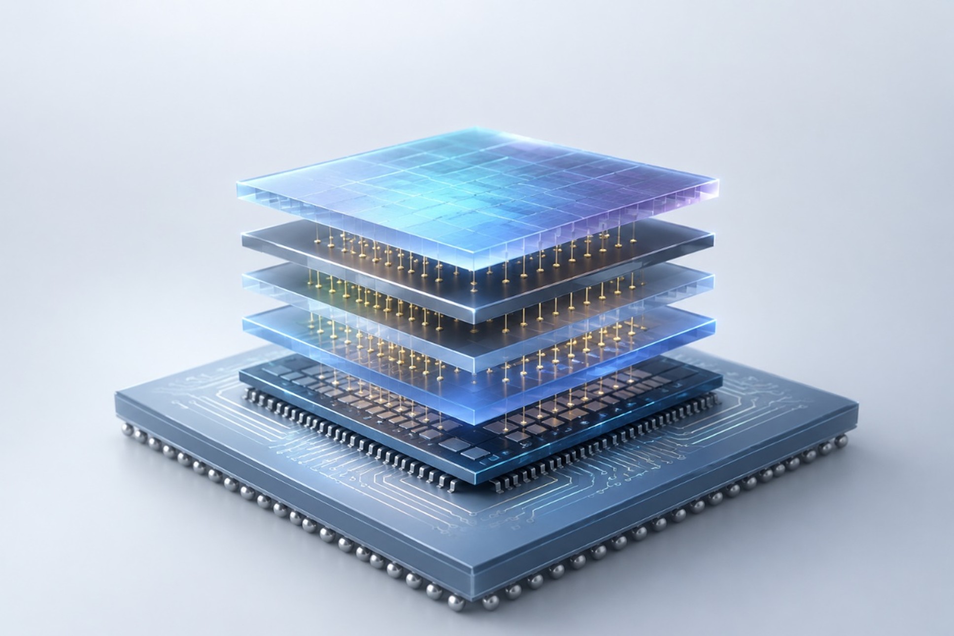
As AI computing demand continues to surge, the semiconductor industry is gradually shifting from a focus on transistor scaling to a new era of system-level stacking and integration. Recently, the industry has been paying close attention to Huawei’s proposed “Tao Law” concept, which emphasizes the use of advanced packaging, chiplets, and multi-die stacking technologies to overcome the limitations of traditional Moore’s Law in process scaling. This signals that the future competitiveness of AI chips will extend beyond transistor density on a single die and increasingly depend on how effectively 3D-IC and heterogeneous integration architectures can improve overall system performance, bandwidth, and power efficiency.
However, as AI chips increasingly adopt vertical stacking architectures involving HBM, high-performance logic dies, and chiplets, testing and repairability have emerged as critical challenges in the advanced packaging era. Given the high value of multi-die packages, discovering memory or interconnect defects after packaging can result in substantial scrap costs. As a result, maintaining testability and repairability within 3D-IC architectures has become an essential issue across the AI semiconductor supply chain.
iSTART-TEK, a company specializing in memory testing and repair technologies, notes that as the industry transitions from Moore’s Law toward stacking-based integration, IEEE 1838 is becoming an indispensable testing standard for 3D-ICs and heterogeneous integration devices. The company has already completed the integration of IEEE 1838 into its memory testing and repair architecture, making it one of the few EDA solution providers capable of delivering comprehensive IEEE 1838 support for memory testing and repair applications.
IEEE 1838 is a testing standard specifically developed for 3D-IC and multi-die stacked architectures. It addresses key challenges such as die-to-die test access, post-stack test path management, and testability within heterogeneous integration environments. While traditional SoC testing primarily targets a single die, the widespread adoption of stacked architectures involving HBM, logic dies, AI accelerators, and chiplets has significantly increased the complexity of test access and fault localization, making IEEE 1838 an increasingly important foundation for advanced packaging technologies.
According to iSTART-TEK, as the industry uses stacking technologies to challenge the limits of Moore’s Law, testing infrastructures must evolve accordingly. In advanced packaging architectures such as CoWoS, 3D-IC, and HBM, the absence of standardized testing mechanisms makes it difficult to efficiently manage multi-die test access and fault diagnosis. Consequently, IEEE 1838 is expected to become a fundamental requirement for future multi-die and heterogeneous integration designs.
Long before 3D-IC technology entered mainstream commercialization, iSTART-TEK had already invested in IEEE 1838-related development and integrated it into its memory testing and repair platform, achieving deep integration with MBIST and BISR architectures. Through the IEEE 1838 framework, the system can preserve SRAM and HBM testing and repair capabilities even after multi-layer stacking is completed, including test path planning, fault localization, repair control, and test access management.
To increase bandwidth and reduce latency, vertical stacking of HBM with GPUs, NPUs, and AI accelerators is rapidly becoming the industry norm, further elevating the importance of memory testing. iSTART-TEK’s IEEE 1838 solution is specifically designed for such heterogeneous integration and high-density stacking scenarios. It supports multi-die test access and memory repair workflows, helping customers maintain high yield and reliability in advanced packaging environments.
In addition, AI devices integrating HBM and high-performance logic dies through CoWoS and 3D-IC architectures represent a significant manufacturing and packaging investment. If memory defects are discovered after packaging and no effective repair mechanism is available, the entire module may need to be discarded. By combining IEEE 1838 with advanced memory repair technologies, iSTART-TEK enables customers to perform precise fault diagnosis and repair even after die stacking has been completed, significantly reducing advanced packaging scrap risks while improving final yield and return on investment (ROI).
Industry observers expect IEEE 1838 to become an increasingly important testing standard throughout the AI semiconductor ecosystem as HBM, chiplets, CoWoS, and heterogeneous integration architectures continue to expand. EDA vendors capable of providing comprehensive memory testing and repair capabilities are expected to play a critical role in the next phase of AI semiconductor competition.
iSTART-TEK emphasizes that it already offers a complete IEEE 1838 memory testing and repair solution, enabling customers to address the testing and yield challenges associated with AI chiplets, HBM, and 3D-IC technologies while preparing for the next generation of advanced packaging opportunities.