1. Relationship Between Read/Write Operations of SRAM Testing Algorithms and SRAM Defect Types
In SRAM testing algorithms, the read and write operations are designed to excite and detect different types of defects. Each operation stresses specific mechanisms in the memory cell or peripheral circuits, thus correlating to specific defect types.
1.1. Write Operations and Related Defects
1.1.1. Purpose
To forcefully set a memory cell to 0 or 1.
1.1.2. Defect Types Detected
-
-
- Stuck-At Faults (SAF)
A cell cannot be written to 0 or 1 because one transistor (pull-up or pull-down) is defective.
Example: If the pull-up PMOS is shorted, even if we try to write a 0, the cell might still stay at 1. - Write Disturb Fault (WDF)
Writing to one cell causes unwanted flipping in an adjacent (victim) cell. - Access Faults
If there are wordline or bitline issues, the write signal might not be correctly delivered. - Open Faults / Resistive Opens
Open faults or resistive opens can cause the write signal to become incomplete.
- Stuck-At Faults (SAF)
-
1.2. Read Operations and Related Defects
1.2.1. Purpose
To sense and verify the stored data.
1.2.2. Defect Types Detected
-
-
- Stuck-At Faults (SAF)
Even if the data was correctly written, if the sensing circuit is defective, the read-out value could still be wrong. - Read Disturb Fault (RDF)
Reading a weak cell might cause its stored value to change unexpectedly due to data loss. - Deceptive Read Destructive Fault (DRDF)
The read operation appears correct, but actually corrupts the stored value silently. - Retention Faults
Reading at different times reveals data retention issues (especially if the cell leaks charge or has a weak latch).
- Stuck-At Faults (SAF)
-
1.3. Combined Read/Write Sequences and Related Defects
Some faults are detectable only through specific sequences of write and read operations, which are illustrated below.
-
- Transition Faults (TF)
This happens when a cell cannot transition correctly from 0 to 1 or from 1 to 0. To detect this, we write a value, read it, then write the opposite value and read again. - Dynamic Faults
This happens when multiple operations (e.g., two writes and two reads) cause failure, which is detected by March tests like March C-, March SS.
- Transition Faults (TF)
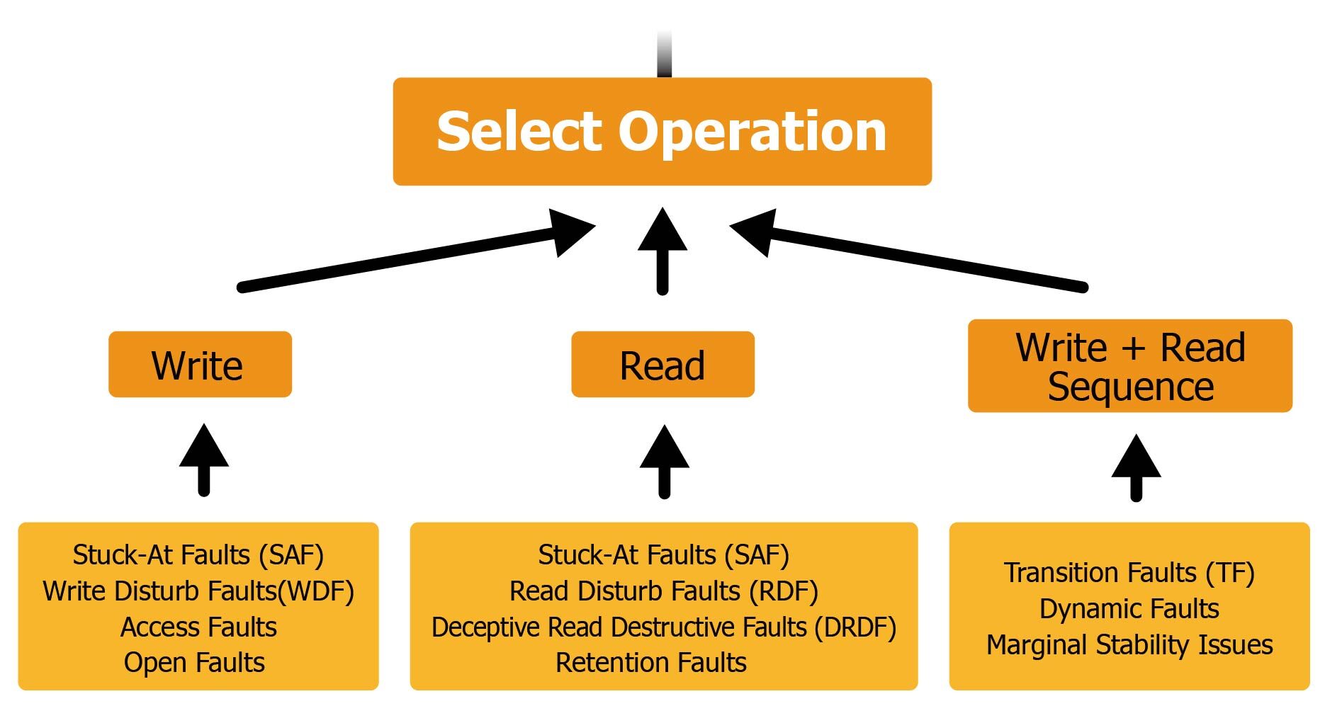
1.4. Summary Table
The operations and faults are summarized as the following table and figure.
| Operation Type | Main Defect Types Detected |
| Write | Stuck-At Faults (SAF), Write Disturb Faults (WDF), Access Faults, and Open Faults |
| Read | Stuck-At Faults (SAF), Read Disturb Faults (RDF), Deceptive Read Destructive Faults (DRDF), and Retention Faults |
| Write and Read Sequence | Transition Faults (TF), Dynamic Faults, and Marginal Stability Issues |
2. SRAM Defect Types vs. Voltage and Temperature
2.1. High Temperature vs. SRAM Behaviors
2.1.1. Read/Write Speed
Higher temperature generally reduces the speed of SRAM due to slower transistor switching. Delay increases because carrier mobility in CMOS transistors decreases as temperature rises.
2.1.2. Leakage Current
SRAM leakage current increases exponentially with temperature. This affects standby power and can destabilize memory cells, especially in deep sub-micron technologies (e.g., 7nm, 5nm).
2.1.3. Data Retention and Stability
SRAM data stability margins (SNM) are degraded at higher temperatures. Increased thermal noise and reduced threshold voltage separation can cause bit flipping or read disturb errors.
2.1.4. High Temperature vs. SRAM Defects
| Aspect | Effect of High Temperature |
| Speed | Decreased (slower switching) |
| Leakage Power | Increased significantly |
| Data Stability | Degraded (lower SNM) |
| Defect Activation | Increased likelihood of failure detection |
| Soft Errors | Higher soft error rate (SER) |
| Aging (NBTI/PBTI) | Faster degradation, long-term failures |
| Electromigration | Increased risk of physical damage |
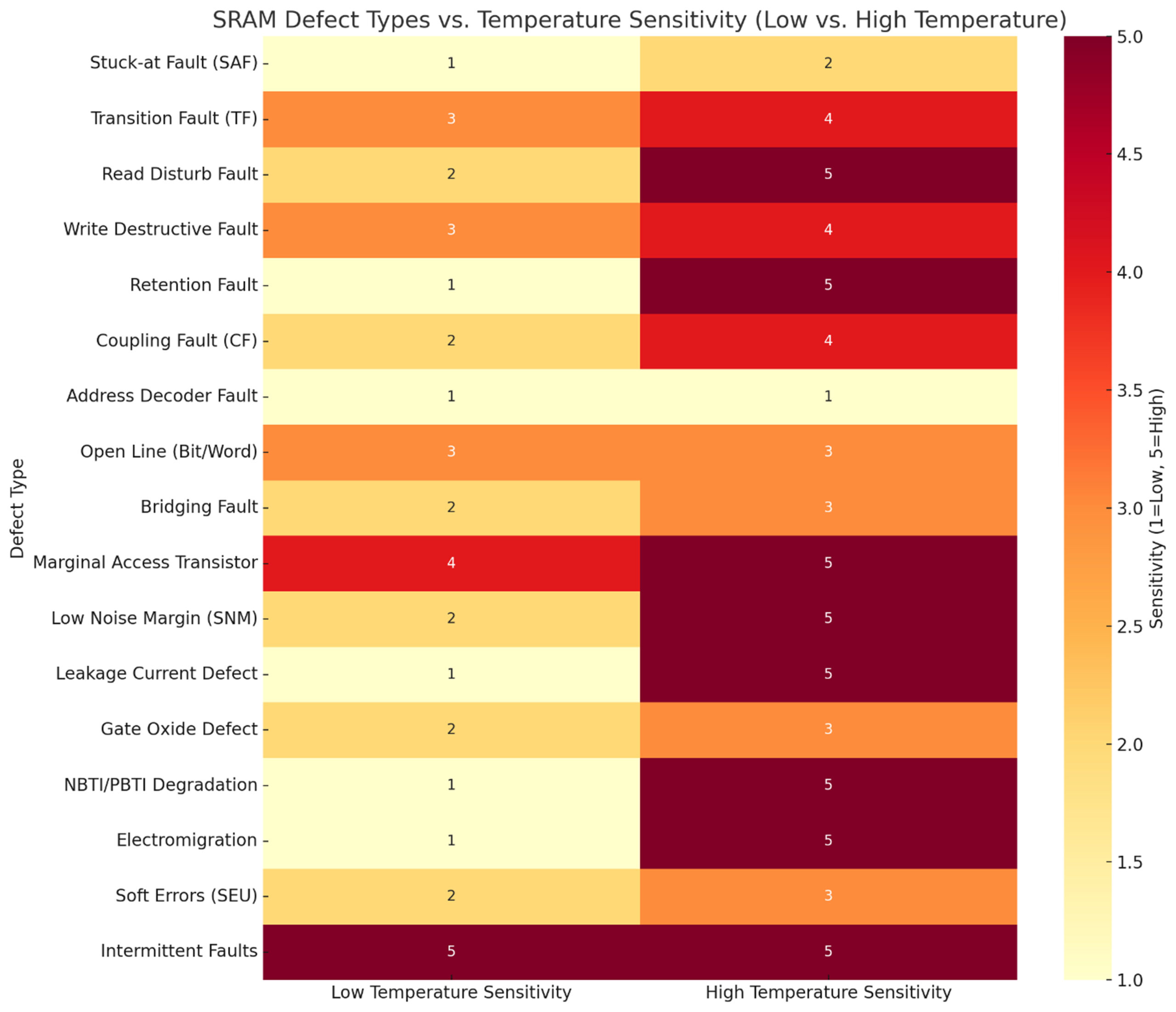
2.1.5. SRAM Defect Types vs. High Temperature
| Defect Type | Temperature Dependency | Effect of High Temperature |
| Stuck-at Fault (SAF) | Low–Medium | May not directly depend on temperature; some marginal SAFs may activate only under temperature stress. |
| Transition Fault (TF) | Medium–High | Higher temperature slows transistor switching → may reveal slow-to-transition defects. |
| Read Disturb Fault | High | Increased thermal noise and reduced noise margin increase chance of read disturb events. |
| Write Destructive Fault | Medium–High | Write margin shrinks with temperature; increases susceptibility to destructive writes. |
| Retention Fault | High | Elevated leakage current and degraded SNM reduce data retention, especially in low-VDD conditions. |
| Coupling Fault (CF) | Medium–High | Thermal expansion and mobility variation may amplify cross-cell interference. |
| Address Decoder Fault | Low | Usually layout/process-related, temperature has minimal direct effect. |
| Open Line (Bit/Word) | Low–Medium | May manifest more clearly at high temperature due to reduced drive strength. |
| Bridging Fault | Medium | Increased leakage may trigger detectable errors in shorts at elevated temperatures. |
| Marginal Access Transistor | High | Delay worsens and noise margin shrinks → failures occur only under hot conditions. |
| Low Noise Margin (SNM) | High | Directly affected — SNM reduces as temperature increases, risking data instability. |
| Leakage Current Defect | Very High | Leakage increases exponentially with temperature → can cause retention loss or disturb. |
| Gate Oxide Defects | Medium–High | Temperature stress may activate latent gate oxide defects. |
| NBTI/PBTI Degradation | High (Long-Term) | Degradation accelerates with heat, leading to aging-induced failures. |
| Electromigration | High (Long-Term) | Driven by high temp and current → causes long-term opens or resistive faults. |
| SEU (Soft Errors) | Medium | Higher temperature increases soft error cross-section slightly (mostly radiation-dependent). |
| Intermittent Faults | Very High | Often only appear under extreme PVT corners (hot, slow, low voltage). |
| Stuck-at Fault (SAF) | Low–Medium | May not directly depend on temperature; some marginal SAFs may activate only under temperature stress. |
| Transition Fault (TF) | Medium–High | Higher temperature slows transistor switching → may reveal slow-to-transition defects. |
High-temperature testing (e.g., burn-in at 125°C) is a common method to activate marginal defects, especially in the following cases.
-
-
- Retention faults
- Write/read disturb
- Transition and coupling faults
-
2.1.6. RAM Defect Types vs. Low Temperature
Low temperature conditions (typically < 0°C to around -40°C) affect various SRAM defect types. While high temperature accelerates many failure mechanisms, low temperature introduces its own unique set of risks—particularly in performance degradation, access instability, and marginal defect activation. The explanation of SRAM defect types vs. low temperature is shown in the table below.
| Defect Type | Effect at Low Temperature | Comment |
| Stuck-at Fault (SAF) | Minimal impact | Usually unrelated to temperature; behavior remains consistent. |
| Transition Fault (TF) | Increased risk due to faster switching and sharp edge transitions | Can expose marginal drive strength or timing defects. |
| Read Disturb Fault | Reduced (higher SNM), but sharp edges may still trigger subtle bit-line effects | May occur less frequently than at high temp. |
| Write Destructive Fault | More likely due to increased drive strength and sharper transitions | Can cause unintentional overwrites if cell is weak. |
| Retention Fault | Improved retention at cold, but marginal Vth shift or weak nodes may cause underdrive | Retention generally improves, but parametric margins can still matter. |
| Coupling Fault (CF) | Slightly reduced risk, but still possible if edge rate is fast | Less crosstalk, but not eliminated. |
| Address Decoder Fault | Minimal effect | Temperature-independent in most cases. |
| Open Line (Bit/Word) | Increased chance of failure activation due to reduced mobility or access transistor underdrive | Delay or non-access issues may appear. |
| Bridging Fault | May remain undetected due to stronger transistor behavior at low temp | Lower leakage can mask bridge effects. |
| Marginal Access Transistor | Higher failure risk due to reduced transistor current in weak access paths | May fail to read/write at cold. |
| Low Noise Margin (SNM) | Improved overall, but mismatch in device strength may still cause flips | Less sensitive to soft errors, but mismatches can create hidden risk. |
| Leakage Current Defect | Greatly reduced leakage → hidden faults may not trigger | Low leakage can mask defects detectable at high temp. |
| Gate Oxide Defects | Less stress activation, but mismatch effects may appear | Fewer charge leaks; long-term reliability not affected. |
| NBTI/PBTI Degradation | Slower degradation | Aging mechanisms suppressed at low temp. |
| Electromigration | Negligible at cold | EM is temperature-accelerated, so low temp has no immediate effect. |
| Soft Errors (SEU) | May increase slightly due to increased device gain | Not major unless radiation is a factor. |
| Intermittent Faults | Very likely to appear, especially in marginal or near-threshold paths | Low temp is often used to expose timing or underdrive issues. |
2.2. SRAM Defect Types vs. Temperature Sensitivity (Low vs. High Temperature)
3. SRAM Defect Types vs. Voltage
The relationship between voltage and SRAM defects is crucial in understanding how static random-access memory (SRAM) behaves under various test conditions. Here’s a breakdown of how voltage affects SRAM and is used to detect or induce defects.
3.1. Voltage Sensitivity of SRAM Cells
SRAM cells rely on precise voltage levels to reliably store and read bits. Defects often affect the noise margin or stability of the cells, which can be exposed through voltage manipulation.
3.1.1. Low Voltage Testing (VLV – Very Low Voltage)
The purpose of this testing is to detect resistive defects (e.g., weak pull-ups or pull-downs) and marginal cells. The reason why it works is that at low voltages, the drive strength of transistors is reduced. Weak or partially defective transistors may fail to flip or hold the correct value.
The detected faults include:
-
-
- Data retention failures
- Read disturb faults
- Access time failures
-
3.1.2. High Voltage Testing (VHV – Very High Voltage)
The purpose of this testing is to expose leakage paths and gate oxide defects. The reason why it works is that high voltage can stress transistors and trigger leakage or breakdown in defective cells.
The detected faults include:
-
-
- Gate oxide shorts
- Leakage between nodes
- Degraded isolation
-
3.2. SRAM-Specific Defect Models and Voltage Interaction
| Defect Type | Effect of Voltage Variation |
| Bridging fault | May manifest under low voltage, as the drive strength can’t overcome the bridge. |
| Open defects | Can cause failure at high voltage due to capacitive effects and charge retention. |
| Soft defects (NBTI, HCI degradation) | More visible at low voltage, affecting timing margins. |
| Read/write disturb faults | Show up under low voltage, where cell stability is more marginal. |
3.3. Effect of Voltage on SRAM Read/Write Margins
The following diagram illustrates how SRAM read and write margins vary with supply voltage.
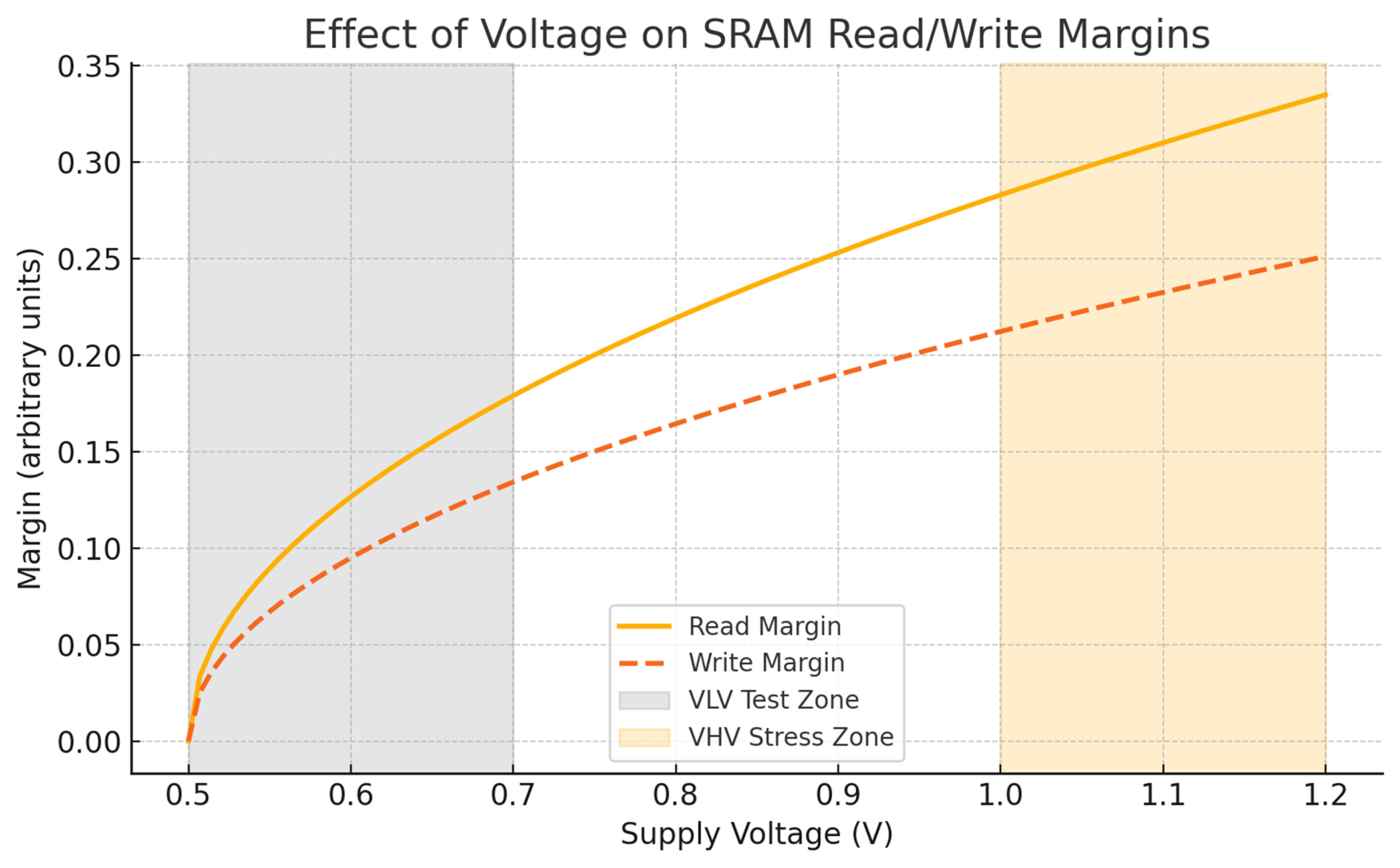
As shown in the diagram, Read Margin increases as voltage rises—cells become more stable. Write Margin also improves with voltage, but remains slightly below the read margin. The gray zone (0.5–0.7 V) represents Very Low Voltage (VLV) testing, where marginal cells are more likely to fail. The orange zone (1.0–1.2 V) indicates Very High Voltage (VHV) stress, useful for exposing leakage or oxide defects.
3.4. High Voltage vs. SRAM Defect Types
| SRAM Defect Type | Effect of High Voltage |
| Gate Oxide Breakdown (GOB) | High voltage accelerates oxide wear, leading to permanent gate oxide damage. |
| Junction Leakage | Increased electric field may enlarge the depletion region, increasing junction leakage. |
| Hot Carrier Injection (HCI) | High voltage can inject carriers into the gate oxide, degrading transistor performance. |
| Time-Dependent Dielectric Breakdown (TDDB) | High voltage reduces oxide reliability, accelerating dielectric breakdown over time. |
| Data Retention Fail (DRF) | Elevated voltage may cause cell instability and charge leakage, impacting retention. |
| Read/Write Disturb Failures | Over-voltage can increase noise margin violations or disturb adjacent cells. |
| Latch-Up | High voltage can trigger parasitic thyristors, causing latch-up conditions. |
| Punch-Through | High voltage can reduce the effective channel length, causing punch-through leakage. |
| Shorts/Bridges | High voltage can damage interconnects or induce metal migration, leading to shorts. |
| Vt Shift (Threshold Voltage Shift) | High voltage stress can cause shifts in transistor threshold, leading to malfunction. |
3.5. Low Voltage vs. SRAM Defect Types
| SRAM Defect Type | Effect of Low Voltage |
| Read Failure | Reduced noise margin makes it harder to distinguish logic states, increasing read failures. |
| Write Failure | Insufficient drive strength to flip the bit cell due to low voltage levels. |
| Access Time Failure | Lower supply voltage increases access time, possibly exceeding timing constraints. |
| Data Retention Failure (DRF) | Marginal cells may not hold state reliably at low voltages. |
| Cell Stability Failure | Reduced cell stability due to decreased static noise margin (SNM). |
| Soft Errors | Cells become more susceptible to noise and radiation-induced errors. |
| Threshold Voltage Variation Sensitivity | Low voltage operation amplifies effects of Vt mismatches, causing failures. |
| Read/Write Disturb Failure | Cells are more prone to disturb from neighboring cells during access operations. |
| Bitline Leakage Failure | Lower voltage reduces the signal swing, increasing sensitivity to leakage. |
| Sense Amplifier Failure | Sense amplifiers may not trigger correctly due to insufficient voltage differential. |
3.6. Voltage Impact on SRAM Defect Types
Below is a comparison table showing how high and low voltages affect various SRAM defect types.
| SRAM Defect Type | High Voltage Effect | Low Voltage Effect |
| Read Failure | Less likely; stronger signal margins. | More likely; reduced noise margins, harder to sense correct value. |
| Write Failure | May overpower adjacent cells or disturb nearby bits. | More likely; weak write strength may not flip cell. |
| Access Time Failure | Faster access time, but could lead to overshoot/glitches. | Slower access; may exceed timing specs. |
| Data Retention Failure (DRF) | Charge leakage or instability due to overstress. | More common due to weak cell holding strength. |
| Cell Stability Failure | Potential overdrive may damage marginal cells. | Less stability due to reduced static noise margin. |
| Gate Oxide Breakdown (GOB) | Very likely; high electric field degrades gate oxide. | Unlikely; electric field too weak to induce breakdown. |
| Junction Leakage | More likely due to increased reverse-bias leakage. | Less likely. |
| Hot Carrier Injection (HCI) | High field causes charge trapping and degradation. | Rare; insufficient energy for carrier injection. |
| TDDB (Time-Dependent Dielectric Breakdown) | Accelerated due to high stress on thin oxides. | Negligible under low field. |
| Punch-Through | High field lowers effective channel length, increasing leakage. | Less concern. |
| Latch-Up | High voltage can trigger latch-up paths. | Not typically triggered under low voltage. |
| Soft Errors | Less likely; better noise immunity. | More likely; weaker noise margins increase vulnerability. |
| Threshold Voltage Shift (Vt Shift) | May be caused by stress or aging at high voltages. | Effects become more noticeable due to reduced VDD/Vt ratio. |
| Sense Amplifier Failure | May overshoot or produce glitches. | May not trigger correctly due to weak signal swing. |
| Bitline Leakage Failure | Metal migration or shorts under prolonged stress. | Weak swing increases sensitivity to leakage. |
4. Voltage Impact on SRAM Defect Types
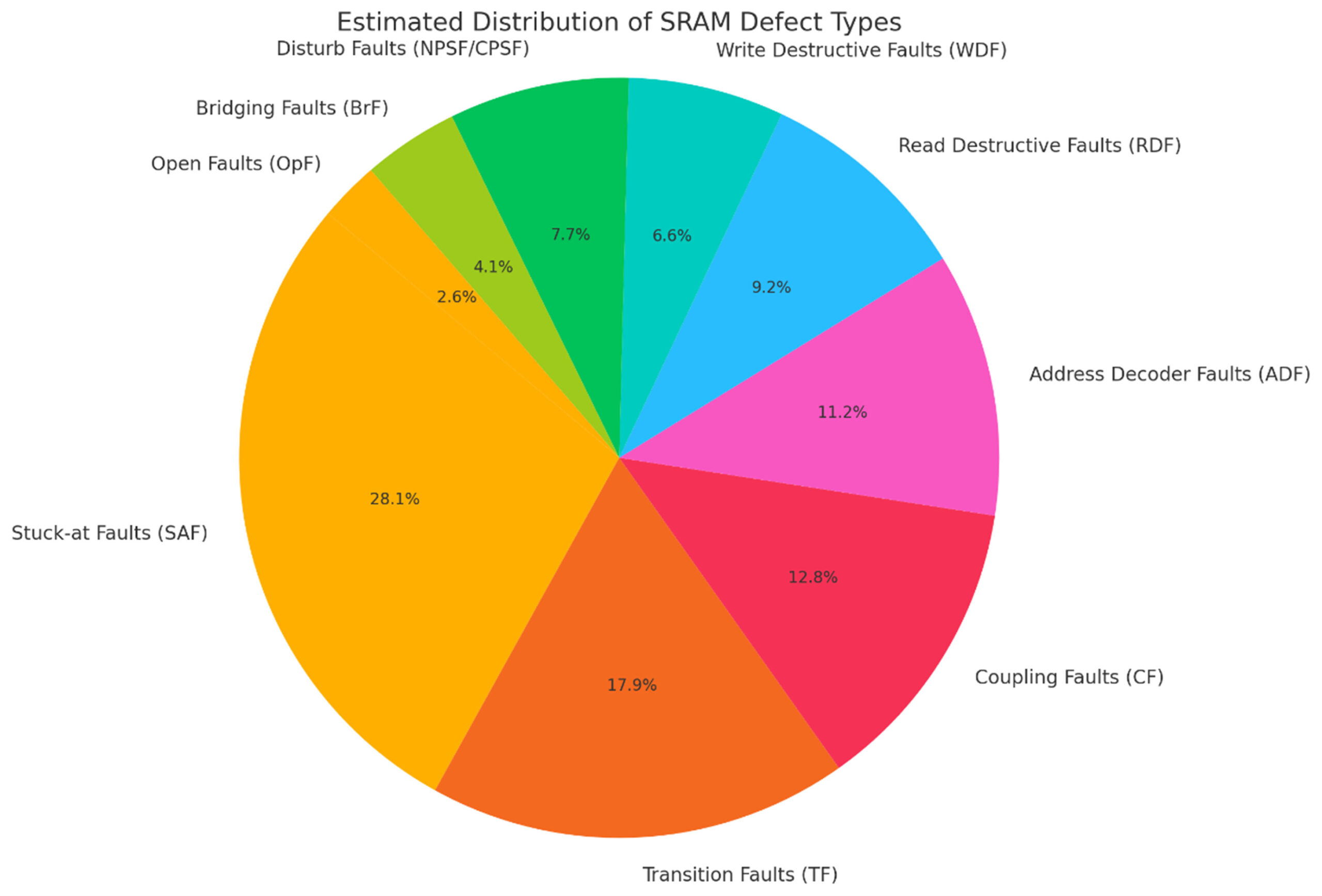
4.1. SRAM Defect Types by Percentage
Below is a typical breakdown of SRAM defect types by percentage, based on common industry data and academic research. These values can vary slightly depending on the process node (e.g., 7nm, 5nm), foundry, and test conditions, but the following is a generalized estimate.
| SRAM Defect Type | Approximate Percentage |
| Stuck-at Faults (SAF) | 25–30% |
| Transition Faults (TF) | 15–20% |
| Coupling Faults (CF) | 10–15% |
| Address Decoder Faults (ADF) | 10–12% |
| Read Destructive Faults (RDF) | 8–10% |
| Write Destructive Faults (WDF) | 5–8% |
| Disturb Faults (e.g., NPSF, CPSF) | 5–10% |
| Bridging Faults (BrF) | 3–5% |
| Open Faults (OpF) | 2–3% |
4.2. MARCH Test Effectiveness for SRAM Defect Types
The table below maps common MARCH test variants to the SRAM defect types that each test is typically effective at detecting.
| March Test | SRAM Defect Types Detected |
| March C- | Stuck-At Faults (SAF), Transition Faults (TF), Address Decoder Faults (ADF), Coupling Faults (CF) |
| March B | SAF, TF, CF (including Inversion and Idempotent), ADF |
| March A | SAF, TF (with better TF detection than March C-), CF |
| March X | SAF, some TF, limited CF |
| March Y | SAF, TF, CF (both inversion and idempotent), improved coverage over March X |
| March LA | SAF, TF, CF, ADF — also targets linked and bridging faults |
| March SS | Detects Write Destructive Faults (WDF), Deceptive Read Destructive Faults (DRDF), SAF, TF |
| March RAW | Focused on detecting Retention Faults (RF), DRDF |
| March LR | Very effective for Low-Power SRAMs; detects SAF, TF, CF, and Retention-related faults |
4.3. MARCH Test Algorithms vs. SRAM Defect Types
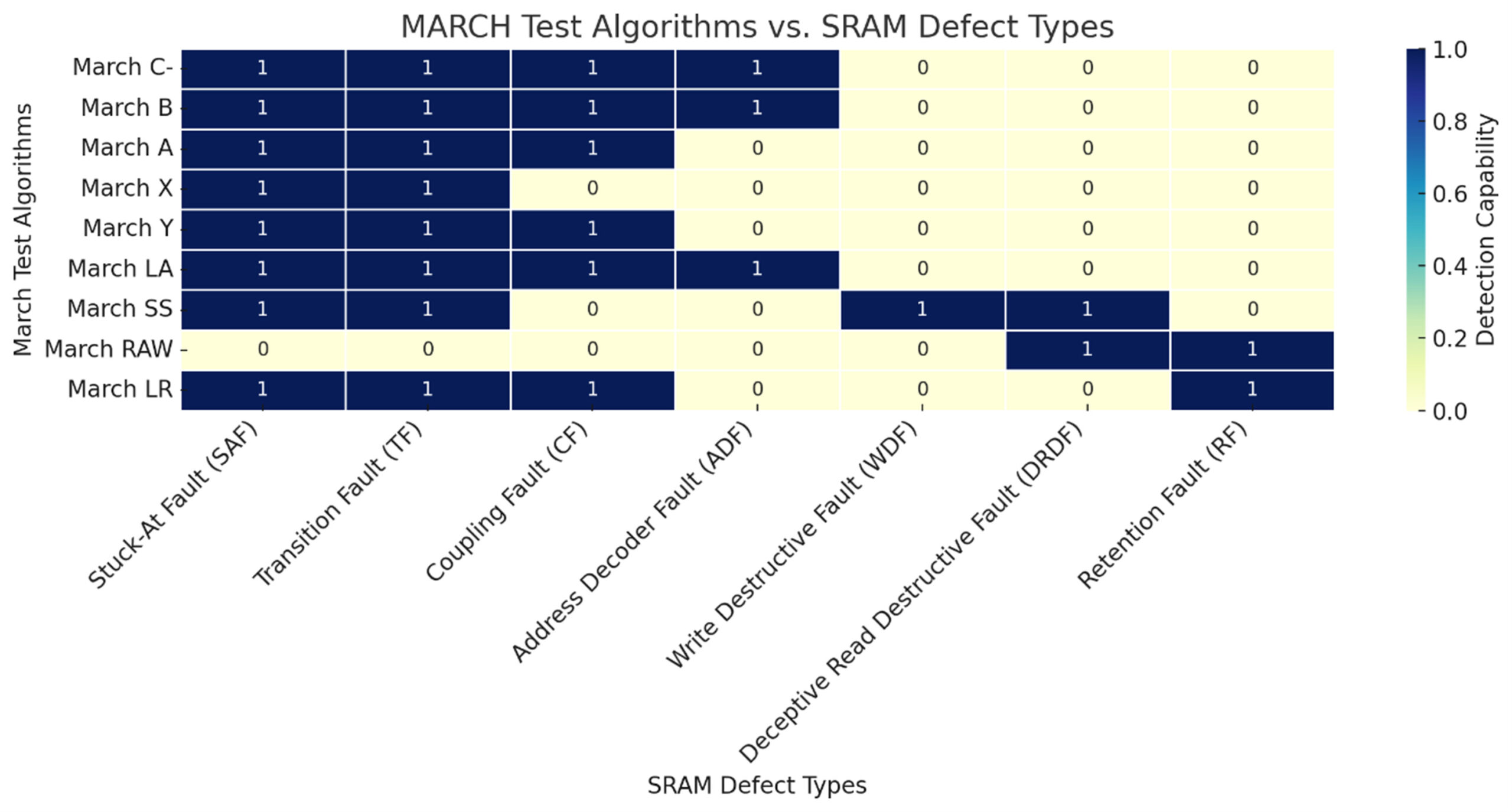
Here is the matrix showing how different MARCH test algorithms detect various SRAM defect types. Detection capability is represented as follows.
-
- 1 (True) = Can detect the fault
- 0 (False) = Not effective for that fault type
4.4. Detection of Dynamic Faults Using March Test Algorithms
Here’s a matrix showing March test algorithms versus their ability to detect dynamic SRAM fault types. Dynamic faults involve timing or sequence-dependent failures that static tests may miss. These typically include Transition Faults (TF), Coupling Faults (CF), and Write Destructive Faults (WDF), among others.
The dynamic fault types cover the following items:
-
- Transition Fault (TF) – cell fails to make 0→1 or 1→0 transition
- Inversion Coupling Fault (CFinv) – writing a value into one cell inverts another
- Idempotent Coupling Fault (CFidem) – writing a value into one cell forces another cell to a fixed value
- Read Destructive Fault (RDF) – read causes data corruption
- Write Destructive Fault (WDF) – write corrupts neighboring or same cell
- Retention Fault (RF) – cell cannot hold value over time
- Dynamic Address Decoder Fault (dADF) – decoder behaves incorrectly based on previous operations
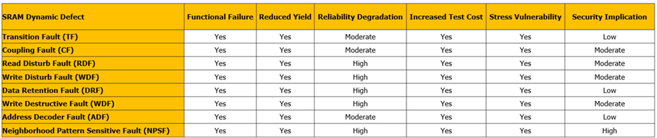
5. The Impact of SRAM Dynamic Defection
The impact of SRAM dynamic defects is significant across functionality, reliability, and yield. These defects may not be caught by simple static tests, yet they degrade performance or cause failure in real-world operations. Below is a structured summary of SRAM dynamic defect impacts.
5.1. Functional Failures
5.1.1. Impact
Incorrect data read/write operations.
5.1.2. Examples
-
-
- Data flip during read or write.
- Random bit errors under high-speed access or stress.
-
5.1.3. Consequence
System crashes, corrupted memory contents, or application errors.
5.2. Reduced Yield
5.2.1. Impact
Chips that pass static tests may fail in real usage scenarios, reducing the number of usable dies.
5.2.2. Cause
Dynamic defects are missed during basic manufacturing tests.
5.2.3. Consequence
Higher test escape rate, increased customer returns (RMA), and poor PPM (parts per million) quality.
5.3. Reliability Degradation
5.3.1. Impact
Memory cells degrade over time, especially with marginal dynamic faults.
5.3.2. Cause
Aging effects (e.g., NBTI, hot-carrier injection), temperature fluctuations, or weak cell margins.
5.3.3. Consequence
Latent faults that worsen with time or usage, leading to in-field failures.
5.4. Test Escapes
5.4.1. Impact
Defective memory cells pass during standard tests (e.g., March C-) but fail under operational conditions.
5.4.2. Cause
Lack of stress-based or timing-sensitive tests (e.g., fails under at-speed access, multi-pattern sequences).
5.4.3. Consequence
Hidden defects shipped to customers.
5.5. Performance Loss
5.5.1. Impact
Memory must operate at reduced speed or with increased guardbanding.
5.5.2. Cause
To mitigate failures, frequency or voltage is reduced.
5.5.3. Consequence
Lower system performance and efficiency.
5.6. Increased Test Time & Cost
5.6.1. Impact
Dynamic fault detection requires more complex and longer test sequences (e.g., March SS, MATS++, BIST with stress modes).
5.6.2. Consequence
Higher cost of test (COT), more expensive ATE (Automatic Test Equipment) time, and possibly added DFT hardware (e.g., MBIST).
5.7. Vulnerability Under Environmental Stress
5.7.1. Impact
Failures only occur under certain voltages or temperatures (e.g., low-VDD, high-temp).
5.7.2. Consequence
Need for multi-corner testing, burn-in, or in-field diagnostics to ensure reliability.
5.8. Security Implications
5.8.1. Impact
Faulty memory may be exploited for fault injection attacks (e.g., fault-based cryptanalysis).
5.8.2. Consequence
Compromised data security or system integrity.
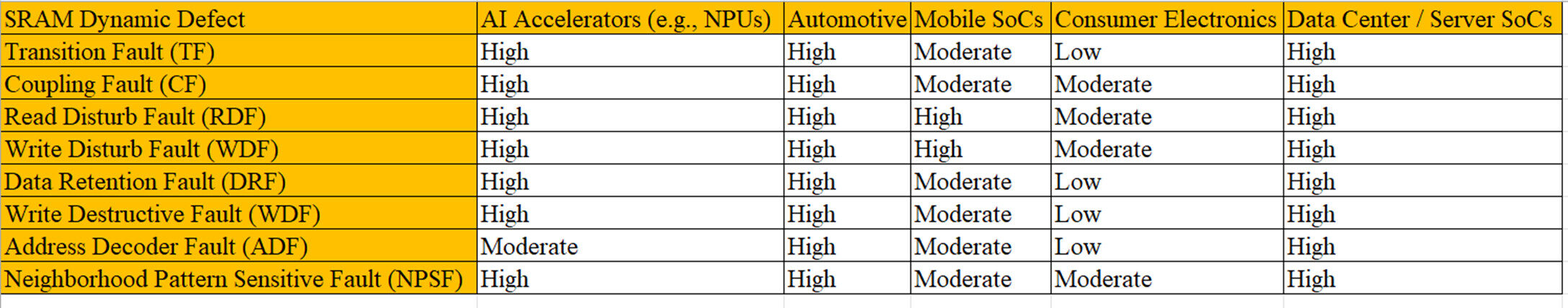
5.9. Application Sensitivity to SRAM Dynamic Defects
6. Use UDA and TEC to Create the Specific SRAM Testing Algorithm
iSTART-TEK’s TEC and UDA can create specific SRAM testing algorithms to detect the above SRAM defects caused by the voltage and temperature. The reasons are illustrated as follows.
- The UDA is a configurable SRAM testing platform that allows users to create specific SRAM testing algorithms by performing consecutive Write and Read operations, and all March test algorithms.ms.
- The TEC can change SRAM testing algorithms after the CP stages based on the LEGO-based SRAM testing elements.
- For example:
- wa, ra, wb, rb, rb,wa, ra, ra, wb, rb, rb, wa, ra, RET, ra, wb, rb, wa, ra, wb, rb, wa, ra
- Detect SRAM defect types
- SAF, TF, CF, ADF, WDF, DRDF, RF
Use UDA and TEC to implement this specific SRAM testing algorithm.